Chapter 14: Semiconductor Electronics: Materials, Devices and Simple Circuits
14.1 Energy Bands in Solids
In a crystal, atoms are closely packed and their electron energy levels interact to form continuous ranges of energy called energy bands.
- Valence Band (VB): The energy band which includes the energy levels of the valence electrons.
- Conduction Band (CB): The energy band above the valence band. When electrons jump to this band, they become free to conduct electricity.
- Energy Band Gap (\(E_g\)): The gap between the top of the VB and the bottom of the CB. No electron can possess an energy level residing in this forbidden gap.

Classification of Materials based on Energy Bands:
- Conductors: In metals, the valence and conduction bands overlap (\(E_g \approx 0\)). Electrons are readily available for conduction.
- Insulators: The valence band is completely full, and the conduction band is completely empty. The energy gap is very large (\(E_g > 3\text{ eV}\)). Very high thermal energy is required to excite an electron across the gap.
- Semiconductors: The valence band is almost full, and the conduction band is almost empty at absolute zero. The energy gap is small (\(E_g < 3\text{ eV}\)). At room temperature, some electrons gain enough thermal energy to jump the gap (e.g., \(E_g \approx 1.1\text{ eV}\) for Si, \(0.72\text{ eV}\) for Ge).
14.2 Intrinsic and Extrinsic Semiconductors
Intrinsic Semiconductors
These are pure semiconductors without any significant impurity (e.g., pure Silicon or Germanium). At absolute zero, they act as perfect insulators. At room temperature, thermally excited electrons jump to the CB, leaving behind positively charged vacancies in the VB called holes.
- Number of electrons (\(n_e\)) = Number of holes (\(n_h\)) = Intrinsic carrier concentration (\(n_i\)).
Extrinsic Semiconductors
To increase conductivity at normal temperatures, deliberate addition of a desirable impurity (doping) is done.
- n-type semiconductor: Created by doping with a pentavalent impurity (Phosphorus, Arsenic). Four valence electrons form covalent bonds, and the fifth weakly bound electron becomes a free charge carrier. Here, electrons are the majority charge carriers (\(n_e \gg n_h\)).
- p-type semiconductor: Created by doping with a trivalent impurity (Boron, Aluminum). One covalent bond is left incomplete, creating a hole. Here, holes are the majority charge carriers (\(n_h \gg n_e\)).
14.3 p-n Junction Formation
When a p-type semiconductor is suitably joined to an n-type semiconductor, the contact surface is called a p-n junction. At the junction, due to the concentration gradient:
- Electrons diffuse from the N-side to the P-side.
- Holes diffuse from the P-side to the N-side. This leaves uncompensated positive ions on the N-side and negative ions on the P-side near the junction. This creates a region devoid of mobile charge carriers, called the depletion region. An electric field develops across this region creating a potential barrier that opposes further diffusion.
14.4 p-n Junction Diode and V-I Characteristics
A p-n junction equipped with metallic contacts is called a semiconductor diode.
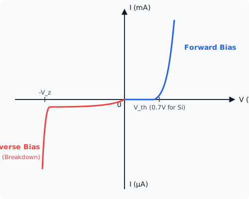
- Forward Bias: When the P-side is connected to the positive terminal and the N-side to the negative terminal of a battery. The applied voltage opposes the barrier potential, reducing the width of the depletion layer. A significant forward current flows exponentially after crossing the cut-in (threshold) voltage.
- Reverse Bias: When the P-side is connected to the negative terminal and the N-side to the positive terminal. The applied voltage supports the barrier potential. The depletion layer widens. Only a minuscule reverse saturation current (\(\mu\text{A}\)) flows due to minority carriers, until the breakdown voltage (\(V_z\)) is reached.
14.5 Application of Junction Diode as a Rectifier
A rectifier is a device that converts Alternating Current (AC) into Direct Current (DC). This application relies on the fact that a p-n junction diode offers very low resistance when forward-biased and extremely high resistance when reverse-biased (unidirectional conduction).
- Half-Wave Rectifier: Uses one diode. It conducts only during the positive half-cycles of the input AC. The output is a pulsating DC with a ripple frequency equal to the input frequency (\(f_{out} = f_{in}\)).
- Full-Wave Rectifier: Uses two diodes with a center-tapped transformer (or four diodes in a bridge). It rectifies both halves of the AC cycle. The output ripple frequency is twice the input frequency (\(f_{out} = 2f_{in}\)).
Competency-Based Questions
Multiple Choice Questions
Q1. [CBSE 2025 Sample Paper] The forbidden energy band gap in conductors, semiconductors, and insulators are \(E_1, E_2,\) and \(E_3\) respectively. The relation among them is:
(A) \(E_1 = E_2 = E_3\)
(B) \(E_1 \lt E_2 \lt E_3\)
(C) \(E_1 > E_2 > E_3\)
(D) \(E_1 \lt E_3 \lt E_2\)
Answer:
Correct Option: (B)
Explanation: Conductors have zero or overlapping band gap (\(E_1 \approx 0\)). Semiconductors have a small band gap (\(E_2 \lt 3\text{ eV}\)). Insulators have a large band gap (\(E_3 > 3\text{ eV}\)). Therefore, \(E_1 \lt E_2 \lt E_3\).
Q2. [CBSE 2021] At absolute zero temperature, a pure silicon crystal:
(A) Works as a superconductor
(B) Works as an insulator
(C) Works as a perfect conductor
(D) Randomly conducts electricity
Answer:
Correct Option: (B)
Explanation: At \(0\text{ K}\), there is absolutely no thermal energy to excite electrons from the valence band to the conduction band. The valence band is completely filled and the conduction band is completely empty. Thus, an intrinsic semiconductor acts as a perfect insulator.
Assertion-Reasoning Type Questions
Q3. [CBSE 2024] Assertion (A): In a p-n junction diode, the width of the depletion layer increases when connected in reverse bias. Reason (R): The reverse bias voltage adds to the built-in potential barrier, pushing the majority carriers away from the junction.
Answer:
Correct Option: (A)
Explanation: In reverse bias, the external battery’s positive terminal is connected to the N-side (attracting electrons away from the junction) and the negative terminal to the P-side (attracting holes away from the junction). This further uncovers immobile lattice ions, widening the depletion region and increasing the overall potential barrier.
Case Study Based Question
Q4. Mobile Phone Chargers (Rectifiers) [CBSE 2023] A standard mobile phone charger essentially functions as an AC to DC converter. The typical electrical grid supplies \(220\text{ V}\) AC voltage, which is far too high and of the wrong type (AC) for a phone battery, which requires \(\sim 5\text{ V}\) DC to charge. The charging brick steps down this voltage using a transformer and then employs a diode-based rectifier circuit, typically a full-wave bridge rectifier with a capacitor filter, to produce a smooth, steady DC voltage.
(i) If the input AC frequency to a full-wave rectifier is \(50\text{ Hz}\), what is the fundamental frequency of the ripples in the output?
(A) \(50\text{ Hz}\)
(B) \(25\text{ Hz}\)
(C) \(100\text{ Hz}\)
(D) \(200\text{ Hz}\)
Answer:
Correct Option: (C) A full-wave rectifier produces two pulses of output per one cycle of AC input. Therefore, the ripple frequency is twice the input frequency (\(2 \times 50 = 100\text{ Hz}\)).
(ii) What is the primary role of the p-n junction diodes in the charger’s rectifier circuit?
(A) To step down the voltage from \(220\text{ V}\) to \(5\text{ V}\)
(B) To amplify the current to charge the battery faster
(C) To act as a one-way valve allowing current to flow in only one direction
(D) To store electrical energy like a capacitor
Answer:
Correct Option: (C) Diodes conduct only during forward bias, rectifying the bidirectional AC current into a unidirectional direct current (DC).